|
微波射频仿真设计 |
|
|
微波射频仿真设计 |
|
| 首页 >> Ansoft Designer >> Ansoft Designer在线帮助文档 |
|
System Simulator > Charge Pump (CPUMP)
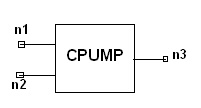
Notes1. This element models the behavior of the charge pump device. 2. Let the first input signal be
3. In the above equation, the term 4. In general, for typical PLL applications, the two input impedances should be set to default (INF), and the output impedance should be set to a large value, normally 1e10 is good enough. Netlist FormCPUMP:Name n1 n2 n3 [I_UP=val] [UP_NFLOOR=val] [UP_FC=val] +[UP_NOISE=val][I_DOWN=val] [DOWN_NFLOOR=val] [DOWN_FC=val] +[DOWN_NOISE=val] [STARTTIME=val] [STOPTIME=val] +[I_TRICKLE=val] [TRICKLE_NFLOOR=val] [TRICKLE_FC=val] +[TRICKLE_NOISE=val] [SEED=val] [RIN1=val] [RIN2=val] +[ROUT=val] Netlist ExampleCPUMP:1 1 2 3 IUP=160uA IDOWN=160uA ITRICKLE=40uA FC=1000Hz
HFSS视频教程 ADS视频教程 CST视频教程 Ansoft Designer 中文教程 |
|||||||||||||||||||||||||||||||||||||||||||||||||||||||||||||||||||||||||||||||||||||||||||||||||||||||||||||||||||||
|
Copyright © 2006 - 2013 微波EDA网, All Rights Reserved 业务联系:mweda@163.com |
|
 , the second input signal be
  , and the output signal
be
, and the output signal
be  , the output signal
is calculated like this:
, the output signal
is calculated like this: 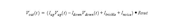
 is formed by two parts: one part is the
noise from the trickle current, the other part is the noise either from
the up current or from the down current depending on which one is active
at that time instance. The user has the option to turn off the noise
for the three noise sources, if any of the noise sources is turned off,
no noise will be generated for that source. Note that noise simulation
is expensive, turning off the noise option will speed up the simulation.
is formed by two parts: one part is the
noise from the trickle current, the other part is the noise either from
the up current or from the down current depending on which one is active
at that time instance. The user has the option to turn off the noise
for the three noise sources, if any of the noise sources is turned off,
no noise will be generated for that source. Note that noise simulation
is expensive, turning off the noise option will speed up the simulation.


