|
微波射频仿真设计 |
|
|
微波射频仿真设计 |
|
| 首页 >> Ansoft Designer >> Ansoft Designer在线帮助文档 |
|
Schematic Editor > S Parameter DefinitionsThere are two common definitions of the scattering matrix, S. One definition is based on traveling waves while the other is based on power waves. Traveling waves correspond to the inward and outward propagating solutions to the telegrapher equations[1]. Power waves relate the power transfer in the inward and outward directions[2,3]. The two definitions are equivalent if the characteristic impedances are real. However if the characteristic impedance is complex, important differences arise.
Both S parameters define the relation between the outgoing waves b and the incoming waves a, or more specifically:  The difference is whether we choose traveling waves or
power waves for a and b. For this derivation we consider
voltage traveling waves. There are also current traveling waves and
many different normalized voltage waves; however, the most common is
the voltage wave:  We will use the subscripts v and p to denote voltage and power waves respectively. If we choose voltage waves, which is typical for high frequency (HF) applications, av and bv are simply:

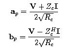
where Zc is a diagonal matrix of comprising the characteristic impedance of each port. The inverse transformation is:  And if we choose power waves, which is typical for circuit applications, ap and bp are:
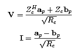
 where Rc is the real part of characteristic impedance, Rc = Re (Zc) and where the superscript H denotes the Hermitian, or conjugate transpose. The inverse transformation of the power waves is:
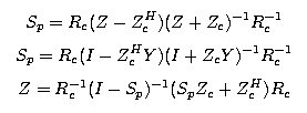
 The voltage based definitions yield the following familiar relationships between the network parameters:
 where

Discussion If the characteristic impedance is completely real (Zc = ZHc = Rc), there is no difference between the two definitions. Only if there is a significant imaginary part to the characteristic impedance will one notice a difference. If there is an imaginary part to the characteristic impedance, the voltage based definition can yield S parameters greater than unity. This occurs if the reactance of the load has the opposite sign of the line, e.g. the load is inductive and the line is capacitive. It is important to note that this is not wrong, just counter-intuitive. If you connect the device to other components within a circuit simulator, you will get the correct answer. There are two significant drawbacks to the power based S parameters[4,5]. A waveguide in cutoff has a characteristic impedance that is completely imaginary (Rc = 0); hence the S parameters are undefined. The concepts of normalized impedance and normalized admittance are not applicable to the power based S parameters; in the numerator we normalize with respect to ZHc , but in the denominator we normalize to Zc. This means that the Smith chart can not be use to convert power based S parameters to the network parameters Y and Z. The Smith chart only works with voltage wave or traveling wave S parameters.
References [1]R. E. Collin, Foundations for Microwave Engineering, New York: McGraw-Hill, 1992. [2]K. Kurokawa, ‘‘Power waves and the scattering matrix,’’ IEEE Trans. Microwave Theory and Tech, pp. 194-202, March 1965. [3]D. Frickey, ‘‘Conversions Between S, Y, Z, h, ABCD, and T Parameters which are valid for complex source and load impedances’’, IEEE Trans. Microwave Theory and Tech, pp. 205-211, February 1994. [4]D. F. Williams and R. Marks, ‘Comments on ‘‘Conversions Between S, Y, Z, h, ABCD, and T Parameters which are valid for complex source and load impedances’’’, IEEE Trans. Microwave Theory and Tech, pp. 914-915, April 1995. [5]R. Marks and D. F. Williams, ‘‘A general waveguide circuit theory,’’ J. Res. Natl. Inst. Stand. Technol., vol. 97, pp.533-561, Sept.-Oct. 1992.
HFSS视频教程 ADS视频教程 CST视频教程 Ansoft Designer 中文教程 |
|
Copyright © 2006 - 2013 微波EDA网, All Rights Reserved 业务联系:mweda@163.com |
|