淘宝官方店     推荐课程     在线工具     联系方式     关于我们  


微波射频仿真设计   Ansoft Designer 中文培训教程   |   HFSS视频培训教程套装


Agilent ADS 视频培训教程   |   CST微波工作室视频教程   |   AWR Microwave Office

          首页 >> Ansoft Designer >> Ansoft Designer在线帮助文档


Ansoft Designer / Ansys Designer 在线帮助文档:


Nexxim Simulator >
Nexxim Component Models >
Transmission Lines >
   W-Model Transmission Line, FIELDSOLVER       

W-Model Transmission Line, FIELDSOLVER

W Fieldsolver Model Netlist Syntax

The netlist format for a W-model transmission line with FIELDSOLVER model type is:

.MODEL modelname W MODELTYPE=FIELDSOLVER

RLGCFILE=filename

ACCURACY=low|medium|high

FDIE=freq

LAYERSTACK=stackname

CONDUCTOR=(

SHAPE=shapename

[MATERIAL=materialname]

[ORIGIN=(x,y)]

[TYPE=SIGNAL|REFERENCE]

)

[CONDUCTOR=(

SHAPE=shapename

[MATERIAL=materialname]

[ORIGIN=(x,y)]

[TYPE=SIGNAL|REFERENCE]

)]...


W FIELDSOLVER Model Parameters

Model Parameter

Description

Unit

Default

LAYERSTACK

Name of layer stack defined in .LAYERSTACK statement

None

Required

CONDUCTOR

Subfields specify the parameters of a conductor. The .MODEL statement can include one or more CONDUCTOR definitions. CONDUCTOR entries must be the last entries in the .MODEL statement

None

One CONDUCTOR definition is required

SHAPE

Name of shape defined in .SHAPE statement

None

Required

MATERIAL

Name of material defined in .MATERIAL statement

None

See description of .MATERIAL statement for default

ORIGIN

In Cartesian coordinates, the (X,Y) location of the origin of the conductor

The X coordinate can be positive, negative, or zero. The Y coordinate must be positive or zero.

Meter

0.0, 0.0

TYPE

Conductor type

SIGNAL = signal node

REFERENCE = use as reference node in W element

None

SIGNAL

RLGCFILE

Name of the file of RLGC values saved for a particular setup. If the file exists, new values are appended.

None

None

ACCURACY

Discretization level for the geometry: low, medium, or high

None

medium

FDIE

Frequency at which dielectric data are specified

Hz

-1e30


Example FIELDSOLVER Model Statement

.MODEL fs_test W MODELTYPE=FIELDSOLVER
+ LAYERSTACK=stack_2
+ RLGCFILE=example4.rlgc
+ ACCURACY=low
+ CONDUCTOR=(SHAPE=rect1, ORIGIN=(-0.6mm, 0.8mm), MATERIAL=copper)
+ CONDUCTOR=(SHAPE=poly_1, ORIGIN=(-0.5mm, 0.2mm), MATERIAL=copper)
+ CONDUCTOR=(SHAPE=strip_1, ORIGIN=(0.1mm, 0.2mm), MATERIAL=copper)
+ CONDUCTOR=(SHAPE=circ_1, ORIGIN=(0.2mm, 0.7mm), MATERIAL=copper)

FIELDSOLVER Model Notes

1. FIELDSOLVER models in externally-generated netlists may contain FSOPTIONS, RLGCFILE, COORD, or OUTPUTFORMAT parameters. These parameters are ignored by this version of Nexxim.

2. The Nexxim fieldsolver uses Cartesian coordinates only. Polar coordinates are not supported.

3. The Nexxim fieldsolver supports conductors of type SIGNAL and REFERENCE. The presence of any conductors of type FLOATING in an externally-generated netlist will cause simulation to fail.

.MATERIAL Statement

The .MATERIAL statement defines the parameters for a single material type. The syntax is:

.MATERIAL materialname METAL|DIELECTRIC

[ER=val]

[CONDUCTIVITY=val]

[LOSSTANGENT=val]

The material must be defined to be either METAL or DIELECTRIC.


MATERIAL Statement Entries

Entry

Description

Unit

Default

ER

Dielectric constant (relative permittivity)

None

METAL: 1

DIELECTRIC: 1

CONDUCTIVITY

Static field conductivity

Siemens/Meter

METAL: -1

DIELECTRIC: 0

LOSSTANGENT

AC field loss tangent of dielectric

None

DIELECTRIC: 0


Example .MATERIAL Statements

.MATERIAL copper METAL CONDUCTIVITY=57.6meg
.MATERIAL diel_1 DIELECTRIC ER=9.64 LOSSTANGENT=0.00064
.MATERIAL diel_2 DIELECTRIC ER=4.95 LOSSTANGENT=0.00086
.MATERIAL diel_3 DIELECTRIC ER=7.80 LOSSTANGENT=0.00024

MATERIAL Statement Notes

1. PEC is a system-defined METAL material with the default values for METAL materials.

2. AIR is a system-defined DIELECTRIC material with the default values for DIELECTRIC materials.

3. The parameter values for these system-defined material names cannot be changed.

.LAYERSTACK Statement

The .LAYERSTACK statement specifies the sequence of dielectric and metal layers in the object to be analyzed. The syntax is:

.LAYERSTACK stackname
[LAYER=(materialname, thickness)
[, LAYER=(materialname, thickness)]...]


LAYERSTACK Statement Entries

Entry

Description

Unit

Default

LAYER

materialname = material name defined in .MATERIAL statement.

thickness = thickness of layer.

Layers are specified starting with the lowest layer.

The bottom of the layer stack is at Y=0.0.

METAL materials can be the bottom layer, the top layer, or both. Inner layers must be DIELECTRIC.

Thickness: Meter

If no LAYER entry is present, stackup represents a free space without a ground plane.

If a LAYER entry is present, the materialname and thickness are both required.


Note 

Nexxim automatically supplies a layer of AIR above the topmost layer specified in the .LAYERSTACK statement. BACKGROUND entries in externally-generated netlists are ignored by Nexxim.

Example .LAYERSTACK Statement

.LAYERSTACK stack_1
+ LAYER=(copper, 0.0) // Lowest layer
+ LAYER=(diel_1, 0.2mm)
+ LAYER=(diel_2, 0.5mm)
+ LAYER=(diel_3, 0.3mm)
+ LAYER=(copper, 0.0) // Topmost layer


.SHAPE Statement

The .SHAPE statement specifies the cross-sectional shape of a conductor. Rectangle, circle, polygon, and strip shapes are supported in Nexxim.

Note 

Externally-generated netlists may include the NH and NW parameters. These parameters are ignored by the Nexxim fieldsolver. The equivalent controls are generated and adjusted internally and do not require user input.


.SHAPE shapename RECTANGLE WIDTH=val HEIGHT=val

The origin for a rectangular conductor is at the lower left corner.


Rectangular SHAPE Statement Entries

Entry

Description

Unit

Default

WIDTH

Width of conductor cross-section

Meter

Required

HEIGHT

Height of conductor cross-section

Meter

Required


.SHAPE shapename CIRCLE RADIUS=val

The origin for a circular conductor is the center of the circle.


Circular SHAPE Statement Entries

Entry

Description

Unit

Default

RADIUS

Radius of conductor cross-section

Meter

Required


.SHAPE shapename POLYGON VERTEX=[x1, y1, x2, y2, ...]

The origin for a polygonal conductor can be any vertex; x1, y1 is recommended.


Polygon SHAPE Statement Entries

Entry

Description

Unit

Default

VERTEX

x and y coordinates of all vertices of the polygon. The vertices may be specified in clockwise or in counterclockwise sequence

Meter

Required


.SHAPE shapename STRIP WIDTH=val

The origin for a 2D strip conductor is the left edge.
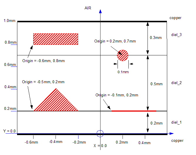


Strip SHAPE Statement Entries

Entry

Description

Unit

Default

Width

Width of conductor

Meter

Required


Example SHAPE Statements

.SHAPE rect_1 RECTANGLE HEIGHT=0.01mm WIDTH=0.4mm
.SHAPE circ_1 CIRCLE RADIUS=0.1mm
.SHAPE poly_1 POLYGON VERTEX=[-0.5,0.2,-0.3,0.4,-0.1,0.2]
.SHAPE strip_1 STRIP WIDTH=0.4mm

Netlist Example of W FIELDSOLVER Transmission Line

Here is an example of a W FIELDSOLVER transmission line that includes all of the statement types described in this topic.

* W FIELDSOLVER TRANSMISSION LINE EXAMPLE

W1 Port1 Port2 0 Port3 Port4 0 N=2 L=10e-3 FSMODEL=fs_test

.MATERIAL copper METAL CONDUCTIVITY=57.6meg
.MATERIAL diel_1 DIELECTRIC ER=9.64 LOSSTANGENT=0.00064
.MATERIAL diel_2 DIELECTRIC ER=4.95 LOSSTANGENT=0.00086
.MATERIAL diel_3 DIELECTRIC ER=7.80 LOSSTANGENT=0.00024

.SHAPE rect_1 RECTANGLE HEIGHT=0.1mm WIDTH=0.4mm
.SHAPE circ_1 CIRCLE RADIUS=0.1mm
.SHAPE poly_1 POLYGON VERTEX=[-0.5,0.2,-0.3,0.4,-0.1,0.2]
.SHAPE strip_1 STRIP WIDTH=0.4mm

.LAYERSTACK stack_1
+ LAYER=(copper, 0.0) // Lowest layer
+ LAYER=(diel_1, 0.2mm)
+ LAYER=(diel_2, 0.5mm)
+ LAYER=(diel_3, 0.3mm)
+ LAYER=(copper, 0.0) // Topmost layer

.MODEL fs_test W MODELTYPE=FIELDSOLVER
+ LAYERSTACK=stack_2
+ RLGCFILE=example4.rlgc
+ ACCURACY=low
+ CONDUCTOR=(SHAPE=rect1, ORIGIN=(-0.6mm, 0.8mm), MATERIAL=copper)
+ CONDUCTOR=(SHAPE=poly_1, ORIGIN=(-0.5mm, 0.2mm), MATERIAL=copper)
+ CONDUCTOR=(SHAPE=strip_1, ORIGIN=(0.1mm, 0.2mm), MATERIAL=copper)
+ CONDUCTOR=(SHAPE=circ_1, ORIGIN=(0.2mm, 0.7mm), MATERIAL=copper)

The transmission line described by this netlist can be diagrammed as:


HFSS视频教学培训教程 ADS2011视频培训教程 CST微波工作室教程 Ansoft Designer 教程

                HFSS视频教程                                      ADS视频教程                               CST视频教程                           Ansoft Designer 中文教程


      Copyright © 2006 - 2013   微波EDA网, All Rights Reserved    业务联系:mweda@163.com