|
微波射频仿真设计 |
|
|
微波射频仿真设计 |
|
| 首页 >> Ansoft Designer >> Ansoft Designer在线帮助文档 |
|
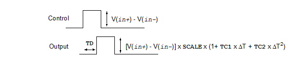
Nexxim Simulator > Voltage-Controlled Voltage Source, Delay
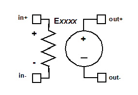 VCVS Delay Netlist FormThe format for a voltage-controlled voltage source with delay is: Exxxx out+ out- [VCVS] DELAY in+ in- TD=val [SCALE=val] [TC1=val] [TC2=val] out+ is the positive node and out- is the negative node of the voltage source. The entry VCVS is the default for the E element type. The entry DELAY selects the E element delay type. in+ and in- are the positive and negative nodes for the control voltage. The figure below diagrams the operation of the VCVS delay element:
VCVS Delay Netlist ExampleE23 outplus outminus VCVS DELAY cplus cminus TD=2.0e-5
HFSS视频教程 ADS视频教程 CST视频教程 Ansoft Designer 中文教程 |
|
Copyright © 2006 - 2013 微波EDA网, All Rights Reserved 业务联系:mweda@163.com |
|


