|
微波射频仿真设计 |
|
|
微波射频仿真设计 |
|
| 首页 >> Ansoft Designer >> Ansoft Designer在线帮助文档 |
|
Nexxim Simulator > PSP 102.1 MOSFET Local Model (Level 69, BINMOD=0, GEOMOD=0)The syntax for a Level 69 PSP102.1 local model MOSFET model is: .MODEL modelname NMOS LEVEL=69 [(][parameter=val] ... [)] or .MODEL modelname PMOS LEVEL=69 [(][parameter=val] ... [)] modelname is the name used by MOSFET instances to refer to this .MODEL statement. The LEVEL=69 entry (plus the parameters BINMOD=0 and GEOMOD=0 on the instance) selects the PSP 102.1 MOSFET local model.
PSP 102.1 Geometry and Stress Dependence Model Equations1 Geometrical Scaling Equations1.1 Effective Length and Width
LEN = 10-6
WEN = 10-6
LE = L - DL = L + DLPS - 2 ´ LAP
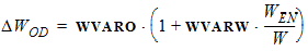
WE = W - DW = W + DWOD - 2 ´ WOT
LE,CV = L + DLPS - 2 ´ LAP + DLQ
WE,CV = W + DWOD - 2 ´ LAP + DWQ
LG,CV = L + DLPS + DLQ
WG,CV = W + DWOD + DWQ
1.2 Process Parameters


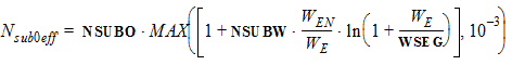
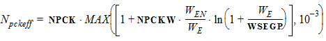
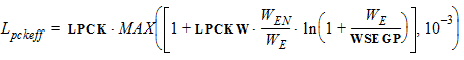
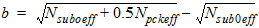
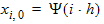
For LE < Lpckeff
For Lpckeff < LE < 2Lpckeff
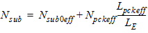
For LE > 2Lpckeff
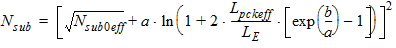
Where: a = 7.5´1010
VNSUB = VNSUBO
NSLPB = NSLPO
DNSUB = DNSUBO


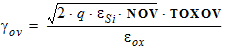
TOXOV = TOXOVO
NOV = DNOVO
1.3 DIBL Parameters
CFB = CFBO
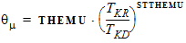
1.4 Mobility Parameters


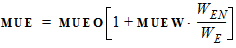
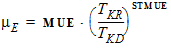
STMUE = STMUEO
THEMU = THEMUO
STTHEMU = STTHEMUO

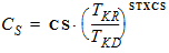
STCS = STCSO

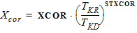
STXCOR = STXCORO
FETA = FETAO
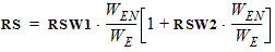
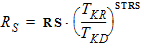
1.5 Series Resistance Parameters
STRS = STRSO
RSB = RSBO
RSG = RSGO
1.6 Velocity Saturation Parameters
THESATB = THESATBO
THESATG = THESATGO
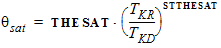
1.7 Saturation Voltage Parameter
1.8 Channel Length Modification (CLM) Parameters
VP = VPO
1.9 Impact Ionization (II) Parameters
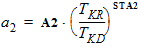
A2 = A2O
STA2 = STA2O

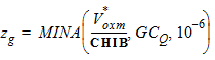
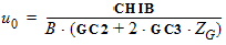
1.10 Gate Current Parameters GCO = GCOO
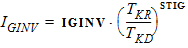
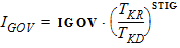
STIG = STIGO
A2 = A2O
GC2 = GC2O
GC3 = GC3O
CHIB = CHIBO
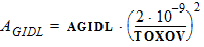
1.11 Gate-Induced Drain Leakage (GIDL) Parameters
BGIDL = BGIDLO
STBGIDL = STBGIDLO
CGIDL = CGIDLO
1.12 Charge Model Parameters

1.12 Noise Model Parameters
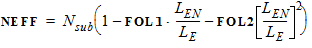
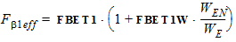
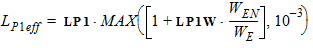
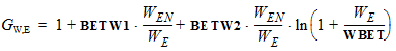
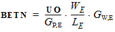
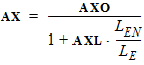
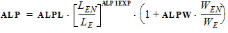
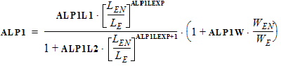
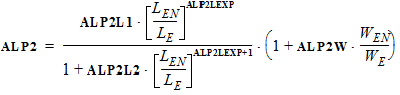
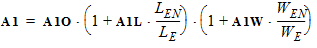
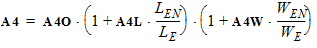
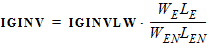
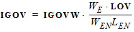
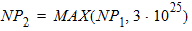
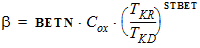
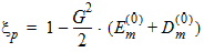
2. Binning Model EquationsWithin a PSP 102.1 model, model parameters are adjusted by the effective channel length and width. There are four types of binning geometry adjustments. The formulas for the adjustment use the following symbols: POx = value of the geometry-independent model parameter “x”, for example POVFB. PLx = value of the length dependence parameter “x”, for example PLVFB. PWx = value of the width dependence parameter “x”, for example PWVFB. PWLx = value of the cross dependence parameter “x”, for example PLWVFB. Le = effective channel length. We= effective channel width. Len = normalized effective channel length. Wen = normalized effective channel width. Type I adjustment: Value = POx+PLx*(Len/Le)+PWx*(Wen/We)+PLWx*(Len/Le)*(Wen/We) Type II adjustment: Value = POx+PLx*(Le/Len)+PWx*(We/Wen)+PLWx*(Le/Len)*(We/Wen) Type III adjustment: Value = POx+PLx*(Len/Le)+PWx*(We/Wen)+PLWx*(Len/Le)*(We/Wen) Type IV adjustment (no binning): Value = POx The parameters that receive Type I adjustments are VFB, STVFB, NEFF, DPHIB, NP, CT, NOV, CF, STBET, MUE, CS, XCOR, RS, THESAT, STTHESAT, THESATB, THESATG, AX, ALP, ALP1, ALP2, A1, A3, A4, NFA, NFB, NFC. The parameters that receive Type II adjustments are IGINV, COX, CGBOV. The parameters that receive Type III adjustments are BETN, IGOV, AGIDL, CGOV, CFR. 2.1 Effective Length and Width for Binning Parameters
LEN = 10-6
WEN = 10-6
LE = L - DL = L + DLPS - 2 ´ LAP
WE = W - DW = W + DWOD - 2 ´ WOT
LE,CV = L + DLPS - 2 ´ LAP + DLQ
WE,CV = W + DWOD - 2 ´ WOT + DWQ
LG,CV = L + DLPS + DLQ
WG,CV = W + DWOD + DWQ
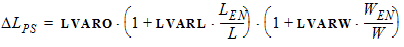
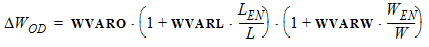
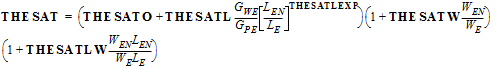
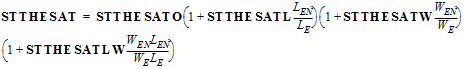
3. Parameter Modifications due to Stress Effects3.1 Layout Effects for Regular Shapes
3.2 Layout Effects for Irregular Shapes
3.3 Calculation of Parameter Modifications
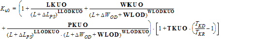

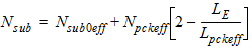
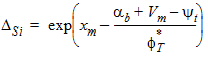
3.3.1 Threshold Voltage Equations
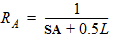
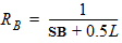
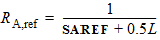
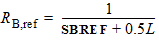
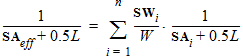
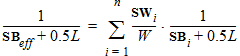
DR = RA + RB - RA,ref - RB,ref
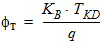
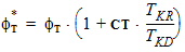
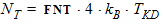
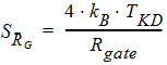
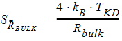
4. Internal Parameters including Temperature Scaling4.1 Transistor Temperature
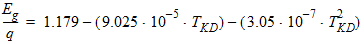
TKR = T0 + TR
TKD = T0 + TA + DTA
DT = TKD -TKR
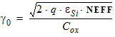
4.2 Local Process Parameters
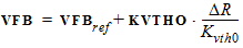
VFB = VFB + STVFB ´ DT


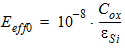
Cox = eox/TOX

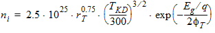
4.3 Polysilicon Depletion Parameters
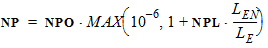
4.3.1 If NP = 0
kP = 0
4.3.2 If NP > 0
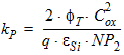
4.4 Quantum-Mechanical Correction Parameters
qlim = 10 fT
For NMOS:
For PMOS:
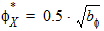
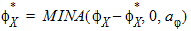
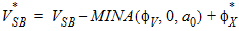
4.5 VSB-Clipping Parameters
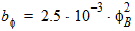
fX = 0.95 ´ fB
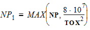
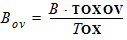
4.6 Local Process Parameters in Gate Overlap Regions

4.7 Mobility Parameters
For NMOS:
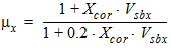
hm = FETA/2
For PMOS:
hm = FETA/3
4.7 Series Resistance Parameters
4.7 Velocity Saturation Parameters
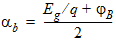
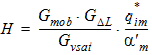
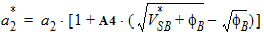
4.8 Impact Ionization Parameters
4.9 Gate Current Parameters

For GC3 < 0:
For GC3 ³ 0:
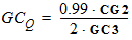
GCQ = 0
4.10 Gate-Induced Drain Leakage (GIDL) Parameters

4.11 Noise Parameters
4.12 Additional Internal Parameters
x1 = 1.25
5. Model Internal Equations
5.1 Conditioning of Terminal Voltages


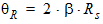
5.1.1 Drain-Induced Barrier Lowering
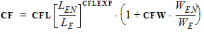
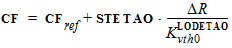
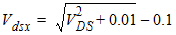
DVG = CF ´ Vdsx ´ (1 + CFB ´ Vsbx)
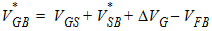

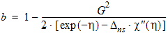
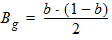
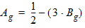
5.2 Bias-Dependent Body Factor

5.3 Surface Potential at Source Side and Related Variables

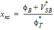
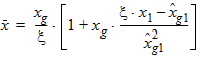
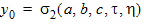
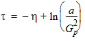
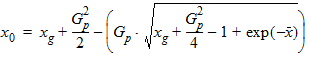
5.3.1 If xg < -xmrg
yg = -xg


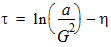
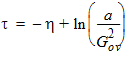
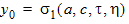
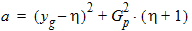
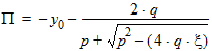
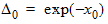
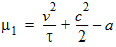
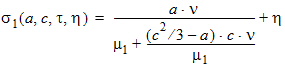
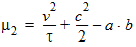
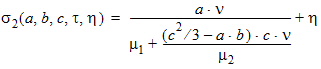
y0 = s1(a, c, t, h)
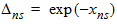
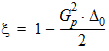
D0 = exp(y0)
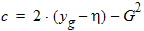
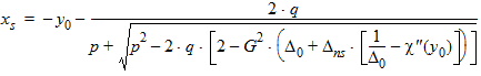
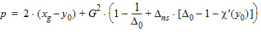
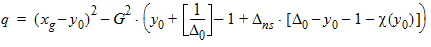
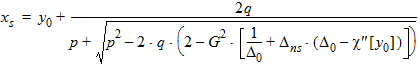
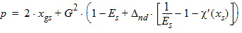
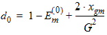
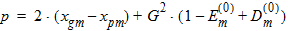
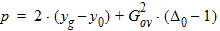
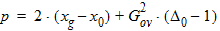
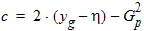
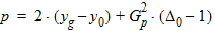
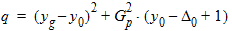
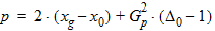
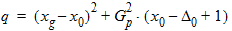
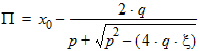
p = 2(yg - y0) + G2(D0 - 1 + Dns[1 - c’(y0) - 1/D0])
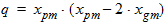
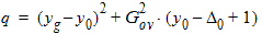
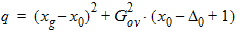
q = (yg - y0)2 + G2(y0 - D0 + 1 + Dns[1 + c’(y0) - 1/D0 - 2y0])
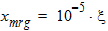
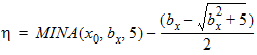
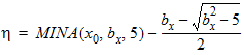
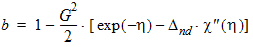
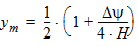
5.3.2 If |xg| £ xmrg
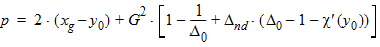
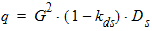
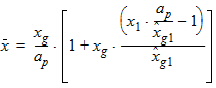
5.3.3 If xg > xmrg

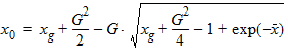
bx = xns + 3
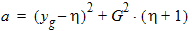
a = (xg - h)2 - G2(exp[-h] + h -1 -Dns[h + 1 + c(h)])

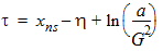
y0 = s2(a, b, c, t, h)
D0 = exp(y0)
5.3.4 For xg > 0
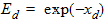
Es = exp(-xs)
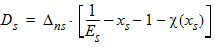
Ps = xs - 1 + Es
5.3.5 For All xg

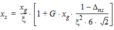
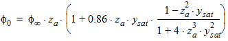
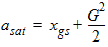
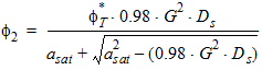
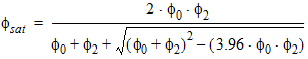
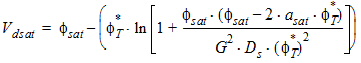
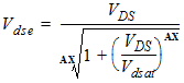
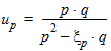
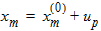
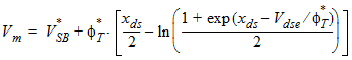
5.4 Drain Saturation Voltage (xg > 0)
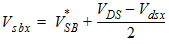
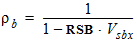
5.4.1 For RSB ³ 0 rb = 1 + RSB ´ Vsbx
5.4.2 For RSB < 0
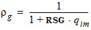
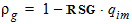
5.4.3 For RSG ³ 0
5.4.4 For RSG < 0
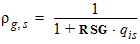
rg,s = 1 - RSG ´ qis
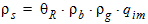
rs = qR ´ rb´ rg,s ´ qis
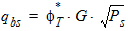
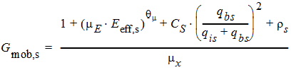
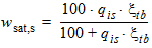
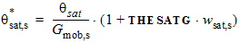
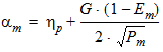
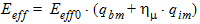
Eeff,s = Eeff0 (qbs + hm ´ qis)
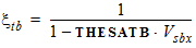
5.4.5 For THESATB ³ 0
xtb = 1 + THESATB ´ Vsbx
5.4.6 For THESATB < 0
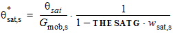
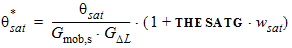
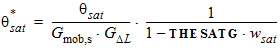
5.4.7 For THESATG ³ 0
5.4.8 For THESATG < 0

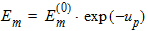
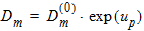
5.4.9 For NMOS
5.4.10 For PMOS
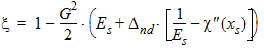
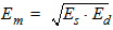
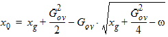
5.4 Surface Potential at Drain Side and Related Variables
5.4.1 For (xg > 0)
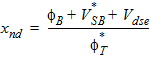
5.4.1.1 If xg £ xmrg
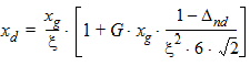
5.4.1.2 If xg > xmrg
bx = xnd + 3.0


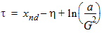

5.4.1.3 For All (xg > 0)
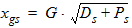
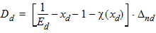
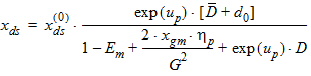
xds = xd - xs
5.4.1.4 If xds < 10-10
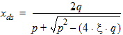
xds = xd + xs
5.4.1.5 For All xds

5.4.1 For All xg

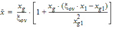
5.5 Mid-Point Surface Potential and Related Variables 5.5.1 If xg > 0


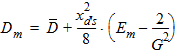
Pm = xm - 1 + Em

5.5.2 If xg £ 0
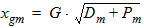
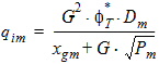
xm = xs
xgm = xg - xs
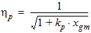
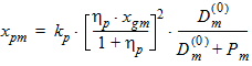
5.6 Polysilicon Depletion The equations in this section are calculated only for kp > 0 and xg > 0 (otherwise hp = 1)


Pm = xm - 1 + Em

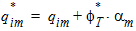
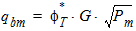
5.6 Potential Midpoint Inversion Charge and Related Variables The equations in this section are calculated only for xg > 0
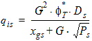
5.6.1 Series Resistance
5.6.1.1 for RSG ³ 0
5.6.1.2 for RSG < 0
5.6.1.3 For All RSG
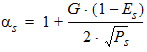
5.6.2 Mobility Reduction
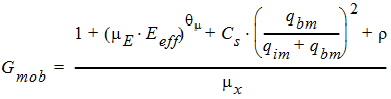
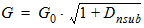
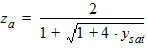
5.6 Drain-Source Channel Current The equations in this section are calculated only for xg > 0 5.6.1 Channel Length Modulation


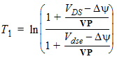
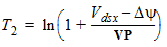
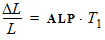
5.6.2 Velocity Saturation
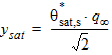
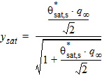
5.6.2.1 For THESATG ³ 0
5.6.2.1 For THESATG < 0
5.6.2.3 For NMOS
5.6.2.3 For PMOS
5.6.2.4 For All THESATG, NMOS and PMOS
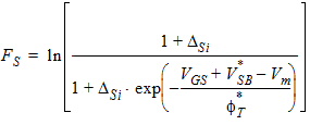
5.6.3 Drain-Source Channel Current
5.6.3.1 For xg £ 0
IDS = 0
5.6.3.2 For xg > 0
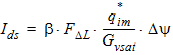
5.6 Auxiliary Variables for Calculating Intrinsic Charges and Gate Current The equations in this section are calculated only for xg > 0
5.7 Impact Ionization or Weak Avalanche The equations in this section are calculated only for SWIMPACT = 1 and xg > 0
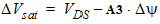
5.7.1 For DVsat £ 0
Mavl = 0
5.7.2 For DVsat > 0
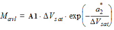
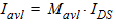
5.7.3 For all DVsat
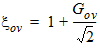
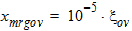
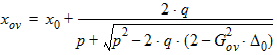
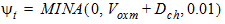
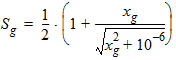
5.7.4 Calculation of xov when xg < -xmrgov
yg = -xg


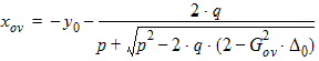
5.7.5 Calculation of xov when | xg | < xmrgov

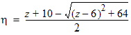
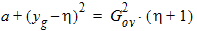
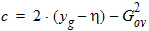
5.7.4 Calculation of xov when xg > xmrgov

5.7.5 For All xg
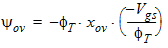

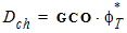
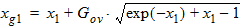
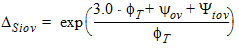
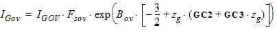
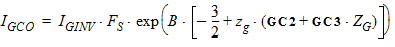
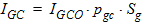
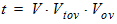
5.8 Gate Current The equations in this section are calculated only when SWIGATE = 1. 5.8.1 Source/Drain Gate Overlap Current
5.8.1.1 Calculation of [IGov(VGX, yov, Vov)]
5.8.1.1.1 zg Calculation For GC3 < 0
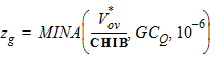
5.8.1.1.2 zg Calculation For GC3 ³ 0

5.8.1.1 Calculation of [IGov(VGX, yov, Vov)], Continued
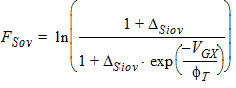
5.8.1.2 Source-Drain Gate Overlap Current, Continued
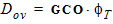
5.8.2 Gate-Channel Current
5.8.2.1 zg Calculation For GC3 < 0
5.8.2.2 zg Calculation For GC3 ³ 0

5.8.2.3 Gate-Channel Current, Continued
5.8.2.4 Calculation of Pgc and Pgd when xg > 0


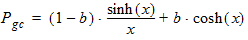
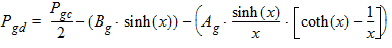
5.8.2.4 Calculation of Pgc and Pgd when xg £ 0
Pgc = 1
Pgd = 1/2
5.8.2.5 Gate-Channel Current, Continued

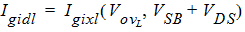
5.9 Gate-Induced Drain/Source Leakage Current The equations in this section are calculated only when SWIGIDL = 1.
5.9.1 Calculation of Igixl(Vov,V)
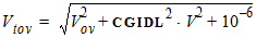
5.9.1.1 For Vov < 0
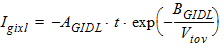
5.9.1.1 For Vov ³ 0
Igixl = 0
5.9.2 Gate-Induced Drain/Source Leakage Current, Continued
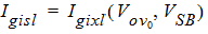
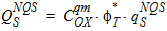
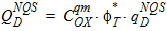
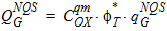
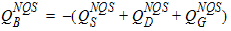
5.10 Total Terminal Currents
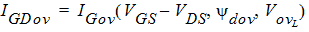
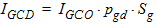
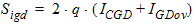
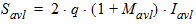
ID = IDS + Iavl - IGDov - IGCD + Igidl
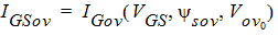
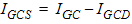
IS = -IDS - IGSov - IGCS + Igisl
IG = IGC + IGB + IGDov - IGSov
IB = -Iavl - IGB - Igidl - Igisl
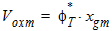
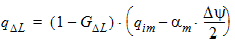
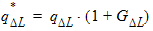
5.11 Quantum-Mechanical Corrections 5.11.1 Calculation of qeff for xg £ 0
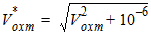
qeff = Voxm
5.11.2 Calculation of qeff for xg > 0
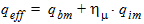
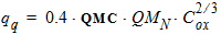
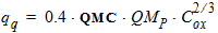
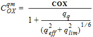
5.11.3 Calculation of COXqm for qq = 0

5.11.4 Calculation of COXqm for qq > 0
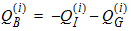
5.12 Intrinsic Charge Model 5.12.1 Calculation of QG(i) , QI(i) , QD(i) for xg > 0

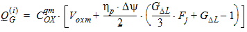
5.12.2 Calculation of QG(i) , QI(i) , QD(i) for xg £ 0


5.12.3 Intrinsic Charge Model, Continued
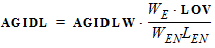
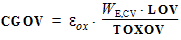
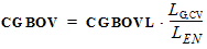
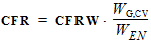
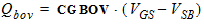
5.13 Extrinsic Charge Model 5.13.1 Source and Drain Overlap Regions
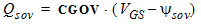

5.13.2 Bulk Overlap Region
5.13.3 Outer Fringe
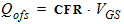
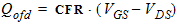
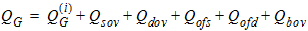
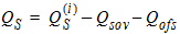
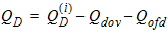
5.14 Total Terminal Charges
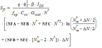
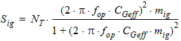
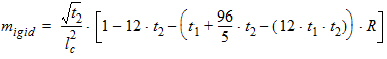
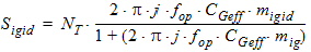
5.15 Noise Model 5.15.1 Flicker Noise Model The equations in this section are calculated only for xg < 0.
fop = operating frequency supplied by the simulator


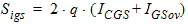
5.15.2 Gate Current Shot Noise
5.15.3 Avalanche Current Shot Noise
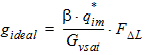
5.15.4 Thermal White Noise of NQS-Model Parasitic resistances
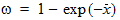
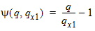
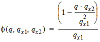
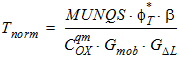
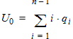
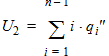
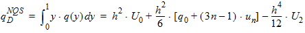
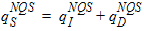
6 NQS Model EquationsNotes: 1. y is the normalized position along the channel (y=0 is the source side, y=1 is the drain side). 2. x is the surface potential (normalized to fT*) at a given position. 6.1 Internal Constants 6.1.1 Internal Constants n and h n = SWNQS + 1 h = 1/n
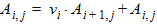
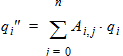
6.1.2 Matrix A (n+1)´(n+1) 6.1.2.1 Initial Values For i = 1 to (n-1): Ai,j = 0 For i = 1 to n: vi = 0 6.1.2.1 First Loop For i = 1 to (n-1):


For j = 0 to n:
6.1.2.2 Second Loop (Back-Substitution) For i = 1 to (n-1): For j = 0 to n:
6.2 Position-Independent Quantities
6.2.1 Calculation of Gp
6.2.1.1 If xg > 0


6.2.1.1 If xg £ 0

Pd = 1
Gp = G
6.2.2 For All Gp

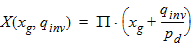
6.3 Position-Dependent Surface Potential and Charge
6.3.1 Interpolated (Quasi-Static) Surface Potential along the Channel:
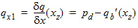
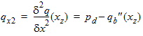
6.3.2 Normalized Bulk Charge and its First Two Derivatives of Surface Potential
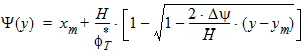
6.3.3 Surface Potential as a Function of Normalized Inversion Charge 6.3.3.1 If xg < -pmrg
yg = - xg


6.3.3.2 If | xg| £ pmrg

6.3.3.3 If xg > xmrg

6.3.4 For all P
6.3.5 Auxiliary Functions
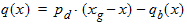
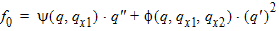
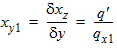
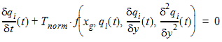
6.3.6 Normalized Right-Hand Side of Continuity Equation [f(xg, q, q' q'')]

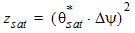
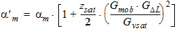
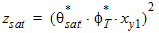
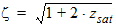
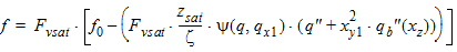
6.3.6.1 Calculation of zsat for NMOS
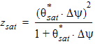
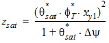
6.3.6.2 Calculation of zsat for PMOS
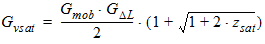
6.3.6.3 For All Zsat

6.3.7 Normalization Constant
6.4 Cubic Spline Interpolation


For 1 £ i £ (n-1)
For 1 £ i £ (n-1)
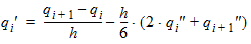
6.5 Continuity Equation

Note: x0,0 = xs and xn,0 = xd
For 1 £ i £ (n-1)

6.6 Non-Quasi-Static Terminal Charges


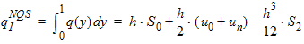
6.6.1 Calculation of qGNQS when SWNQS is odd (1, 3, 5, or 9)
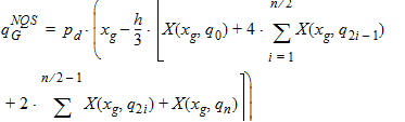
6.6.1 Calculation of qGNQS when SWNQS is 2

6.6.2 Conversion to Conventional Units
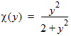
7 Auxiliary Equations7.1 Smoothing Functions
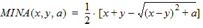
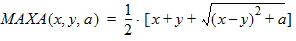
7.2 Surface Potential Approximation Functions

HFSS视频教程 ADS视频教程 CST视频教程 Ansoft Designer 中文教程 |
|
Copyright © 2006 - 2013 微波EDA网, All Rights Reserved 业务联系:mweda@163.com |
|