淘宝官方店     推荐课程     在线工具     联系方式     关于我们  


微波射频仿真设计   Ansoft Designer 中文培训教程   |   HFSS视频培训教程套装


Agilent ADS 视频培训教程   |   CST微波工作室视频教程   |   AWR Microwave Office

          首页 >> Ansoft Designer >> Ansoft Designer在线帮助文档


Ansoft Designer / Ansys Designer 在线帮助文档:


Nexxim Simulator >
Nexxim Component Models >
MOSFET Levels 49 through 54 >
   MOSFET Instance, BSIM4 Model (Level 54)       

MOSFET Instance, BSIM4 Model (Level 54)


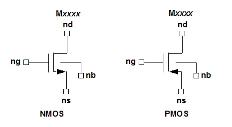
This level implements the University of California, Berkeley, BSIM4.3.0 MOSFET model.

BSIM4 MOSFET Instance Netlist Syntax

The syntax for a LEVEL=54 BSIM4 MOSFET instance is:

Mxxxx nd ng ns [nb] modelname [L=length] [W=width]

[ACNQSMOD=val] [AD=val] [AS=val] [GEO=val] [GEOMOD=val]

[M=val] [MIN=val] [NF=val] [NRD=val] [NRS=val]

[PD=val] [PS=val]

[RBODYMOD=val] [RGATEMOD=val] [RGEOMOD=val] [TRNQSMOD=val]

[RBDB=val] [RBPB=val] [RBPD=val] [RBPS=val] [RBSB=val]

[SA=val] [SB=val] [SD=val] [MULU0=val] [DELVTO=val]

[TNOM=val] [DTEMP=val] [SCALE=val]

[OFF=val] [ICVDS=val] [ICVGS=val] [ICVBS=val]

[RDC=val] [RSC=val] [SCA=val] [SCB=val] [SCC=val] [SC=val] [XGW=val] [NGCON=val]

nd is the drain node, ng is the gate node, ns is the source node, and nb is the bulk or substrate node of the MOSFET. modelname is the name of a BSIM4 MOSFET model defined in a .MODEL statement elsewhere in the netlist.

When the option WL is in effect (on the .OPTION statement), the syntax becomes:

Mxxxx nd ng ns [nb] modelname [width] [length]

[ACNQSMOD=val] [AD=val] [AS=val] [GEO=val] [GEOMOD=val]

[M=val] [MIN=val] [NF=val] [NRD=val] [NRS=val]

[PD=val] [PS=val]

[RBODYMOD=val] [RGATEMOD=val] [RGEOMOD=val] [TRNQSMOD=val]

[RBDB=val] [RBPB=val] [RBPD=val] [RBPS=val] [RBSB=val]

[SA=val] [SB=val] [SD=val] [MULU0=val] [DELVTO=val]

[TNOM=val] [DTEMP=val] [SCALE=val]


Level 54 MOSFET Instance Parameters

Instance Parameter

Description

Unit

Default

ACNQSMOD

AC small-signal NQS model selector

None

0

AD

Drain diffusion area

Meter2

0

AS

Source diffusion area

Meter2

0

DELVTO

Shift in VTH0

Volt

0.0

DTEMP

Difference between device and circuit temperature

NOTE: DTEMP is supported only in netlists for Release 3.5.

°C

0.0

GEOMOD

Geometry-dependent parasitics model selector, specifying how the end source/drain diffusions are connected

0 = Isolated

1 = shared drain

2 = shared source

3 = shared source and drain

None

0 (isolated)

ICVBS

Initial Vbs voltage

Volt

0

ICVDS

Initial Vds voltage

Volt

0

ICVGS

Initial Vgs voltage

Volt

0

L

Physical gate length

Meter

5.0e-6

M

Multiplier: simulates parallel transistors

None

1.0

MIN

Flag to minimize the number of drain or source diffusions for even-fingered device

None

0

MULU0

Mobility multiplier

None

1.0

NF

Number of device fingers

None

1

NGCON

Number of gate contacts

None

1

NRD

Number of drain diffusion squares

Square

1

NRS

Number of source diffusion squares

Square

1

OFF

Flag to indicate that device is initially off

None

0

PD

Drain diffusion periphery

Meter

0

PS

Source diffusion periphery

Meter

0

RBDB

Resistance connected between dbNode and bNode

Ohm

50.0

RBODYMOD

Substrate resistance network model selector

0 = Network off

None

0

RBPB

Resistance connected between bNodePrime and bNode

Ohm

50.0

RBPD

Resistance connected between bNodePrime and dbNode

Ohm

50.0

RBPS

Resistance connected between bNodePrime and sbNode

Ohm

50.0

RBSB

Resistance connected between sbNode and bNode

Ohm

50.0

RDC

Drain contact resistance

Ohm

0

RGATEMOD

Gate resistance model selector

0 = No gate resistance

None

0

RGEOMOD

Source/drain diffusion resistance and contact model selector

None

0 (no source/drain diffusion resistance

RSC

Source contact resistance

Ohm

0

SA

Distance from OD edge to poly on one side

Meter

0.0

SB

Distance from OD edge to poly on other side

Meter

0.0

SC

Distance to a single edge

Meter

0

SC

Distance to a single edge

Meter

0.0

SCA

Integral of the first distribution function for scattered well dopant

None

Calculated

SCA

Integral of the first distribution function for scattered well dopant


SCALE

Element scaling parameter

None

1.0

SCB

Integral of the second distribution function for scattered well dopant

None

Calculated

SCB

Integral of the second distribution function for scattered well dopant


SCC

Integral of the third distribution function for scattered well dopant

None

Calculated

SCC

Integral of the third distribution function for scattered well dopant


SD

Distance between neighboring fingers

Meter

0.0

TNOM

Temperature at which parameters are extracted

°C

25

TRNQSMOD

Transient NQS model selector

None

0 (Off)

W

Physical gate width

Meter

5.0e-6

XGW

Distance from the gate contact to the channel edge

Meter

0.0


BSIM4 MOSFET Instance Netlist Example

M1 10 11 12 mosfet54

M12 G3 VDD 0 0 mosfet54 M=2 DTEMP=30


HFSS视频教学培训教程 ADS2011视频培训教程 CST微波工作室教程 Ansoft Designer 教程

                HFSS视频教程                                      ADS视频教程                               CST视频教程                           Ansoft Designer 中文教程


      Copyright © 2006 - 2013   微波EDA网, All Rights Reserved    业务联系:mweda@163.com