|
 Ansoft Designer / Ansys Designer 在线帮助文档: Ansoft Designer / Ansys Designer 在线帮助文档:
Nexxim Simulator >
Nexxim Component Models >
FETs (JFETs and MESFETs) >
MESFET, Materka Model (Level 24)
The .MODEL statement for the Level
24 Materka MESFET models specifies values for one or more model parameters.
.MODEL modelname NJF LEVEL=24
[modelparameter=]val] ...
or
.MODEL modelname PJF LEVEL=24
[modelparameter=]val] ...
LEVEL=24 specifies
the Materka MESFET model.
Level 24 Materka MESFET
Model Parameters
Model Parameter
|
Description
|
Unit
|
Default
|
LEVEL
|
24 is required to select the Materka
MESFET model
|
None
|
1 (default if LEVEL parameter is
omitted)
|
AF
|
Flicker noise exponent
|
None
|
1.0
|
CDS
|
Drain-source capacitance
|
Farad
|
0.0
|
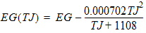
EG
|
Barrier height at 0°K (CAP model)
|
Volt
|
0.8
|
FCP
|
Coefficient for forward-bias depletion
capacitance formulas
|
None
|
1.0
|
GAMA
|
Drain voltage-induced threshold
voltage lowering coefficient
|
None
|
0.0
|
IDSS
|
Drain saturation current for Vgs=Vgss
|
Ampere
|
0.1
|
KFN
|
Flicker noise coefficient
|
None
|
0.0
|
RD
|
Drain ohmic resistance
|
Ohm
|
0.0
|
RG
|
Gate ohmic resistance
|
Ohm
|
0.0
|
RS
|
Source ohmic resistance
|
Ohm
|
0.0
|
TNOM
|
Nominal circuit temperature
|
°C
|
25.0
|
VP0
|
Threshold voltage
|
Volt
|
-2.0
|
XTI
|
Saturation current temperature
exponent
|
None
|
2.0
|
EE (E)
|
Constant part of power law parameter
|
None
|
2.0
|
KE
|
Dependence of power law on Vgs
|
None
|
0.0
|
SL
|
Slope of the Vgs=0 drain characteristic
in the linear region
|
None
|
0.15
|
KG
|
Drain dependence on Vgs in the
linear region
|
None
|
0.0
|
SS
|
Slope of the drain characteristic
in the linear region
|
None
|
0.0
|
T
|
Channel transit time delay
|
Second
|
0.0
|
DLVL
|
Model selector: 0 = Diode model,
1 = Raytheon model
|
None
|
0
|
IG0
|
Diode saturation current
|
Ampere
|
0.0
|
AFAG
|
Slope factor for diode saturation
current
|
None
|
38.696
|
IB0
|
Breakdown saturation current
|
Ampere
|
0.0
|
AFAB
|
Slope factor for breakdown saturation
current
|
None
|
0.0
|
VBC
|
Breakdown voltage
|
Volt
|
None
|
GMAX
|
Breakdown conductance
|
Siemen
|
0.0
|
K1D
|
Fitting parameter
|
None
|
0.0
|
K2D
|
Fitting parameter
|
None
|
0.0
|
K3D
|
Fitting parameter
|
None
|
0.0
|
R10
|
Intrinsic channel resistance for
Vgs=0
|
Ohm
|
0.0
|
KR
|
Slope factor of intrinsic channel
resistance
|
None
|
0.0
|
CLVL
|
Capacitance model selector:
1 = Materka model,
2 = Raytheon model
|
None
|
1
|
CDSD
|
Low-frequency trapping capacitance
|
Farad
|
0.0
|
RDSD
|
Channel trapping resistance
|
Ohm
|
None
|
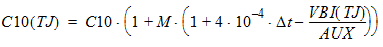
C10
|
Gate-source Schottky barrier capacitance
for Vgs=0
|
Farad
|
0.0
|
K1
|
Slope parameter for gate-source
capacitance
|
None
|
1.25
|
MGS
|
Gate-source grading coefficient
|
None
|
0.5
|
C1S
|
Constant parasitic component of
gate-source capacitance
|
Farad
|
0.0
|
CF0
|
Gate-drain feedback capacitance
|
Farad
|
0.0
|
KF
|
Slope parameter for gate-drain
capacitance
|
None
|
1.25
|
MGD
|
Gate-drain grading coefficient
|
None
|
0.5
|
FCC
|
Forward-bias depletion capacitance
coefficient
|
None
|
0.8
|
CGS0
|
Gate-source Schottky barrier capacitance
for Vgs=0
|
Farad
|
0.0
|
CGD0
|
Gate-drain Schottky barrier capacitance
for Vgs=0
|
Farad
|
0.0
|
VBI
|
Built-in barrier potential for
Raytheon capacitance model
|
Volt
|
0.8
|
RI
|
Channel resistance for Raytheon
capacitance model
|
Ohm
|
0.0
|
VMAX
|
Maximum voltage used for Vnew
|
Volt
|
0.5
|
VDELTA
|
Capacitance transition voltage
|
Volt
|
0.2
|
TMOD
|
Temperature model selector:
0 = quadratic, 1 = linear
|
None
|
0
|
AVT0
|
Vp0 linear temperature coefficient
|
None
|
0.0
|
ARI
|
RI linear temperature coefficient
|
None
|
0.0
|
ARG
|
RG linear temperature coefficient
|
None
|
0.0
|
ARD
|
RD linear temperature coefficient
|
None
|
0.0
|
ARS
|
RS linear temperature coefficient
|
None
|
0.0
|
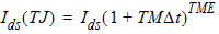
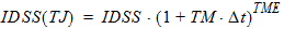
TM
|
IDS linear temperature coefficient
|
None
|
0.0
|
TME
|
IDS power law temperature coefficient
|
None
|
0.0
|
M
|
Capacitance model grading coefficient
(Note: This parameter M does not override the instance scaling parameter
M)
|
None
|
0.5
|
BVT0
|
Vp0 quadratic temperature coefficient
|
None
|
0.0
|
BRI
|
RI quadratic temperature coefficient
|
None
|
0.0
|
BRG
|
RG quadratic temperature coefficient
|
None
|
0.0
|
BRD
|
RD quadratic temperature coefficient
|
None
|
0.0
|
BRS
|
RS quadratic temperature coefficient
|
None
|
0.0
|
AIDS
|
IDSS linear temperature coefficient
|
None
|
0.0
|
AGAM
|
GAMA linear temperature coefficient
|
None
|
0.0
|
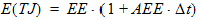
AEE
|
EE linear temperature coefficient
|
None
|
0.0
|
AKE
|
KE linear temperature coefficient
|
None
|
0.0
|
ASL
|
SL linear temperature coefficient
|
None
|
0.0
|
AKG
|
KG linear temperature coefficient
|
None
|
0.0
|
ASS
|
SS linear temperature coefficient
|
None
|
0.0
|
AT
|
T linear temperature coefficient
|
None
|
0.0
|
AC10
|
C10 linear temperature coefficient
|
None
|
0.0
|
ACF0
|
CF0 linear temperature coefficient
|
None
|
0.0
|
AVBC
|
VBC linear temperature coefficient
|
None
|
0.0
|
ACGS
|
CGS linear temperature coefficient
|
None
|
0.0
|
ACGD
|
CGD linear temperature coefficient
|
None
|
0.0
|
AVBI
|
VBI linear temperature coefficient
|
None
|
0.0
|
AGMX
|
GMAX linear temperature coefficient
|
None
|
0.0
|
SN
|
Noise analysis selector, 1=on,
0=off
|
None
|
1
|
RGS
|
Gate-source ohmic resistance for
Enhanced Raytheon model
|
Ohm
|
0.0
|
RGD
|
Gate-drain ohmic resistance for
Enhanced Raytheon model
|
Ohm
|
0.0
|
Materka MESFET Model Netlist Example
.MODEL mesfet24 NJF LEVEL=24
+ idss=0.0649003 alpha1=1.5 gama=-0.0306278
Device Equations
Vgsi = Intrinsic
gate-source voltage
Vdsi = Intrinsic
drain-source voltage
Vgdi = Intrinsic
gate-drain voltage
V1 = Voltage across Cgs and Ri
Vt = Thermal
voltage k TJ/q
k = Boltzmann’s constant
q = Electron charge
TJ = Analysis temperature, Kelvin
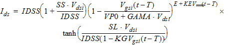
Channel Current
![[spacer]](1p.gif)
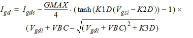
Diodes

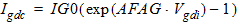
When DLVL = DIOD

When DLVL = RAY
Channel Resistance
When KR*Vgsi < 1.0
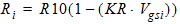
When KR*Vgsi >= 1.0
Ri
= 0
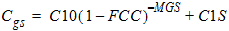
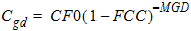
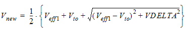
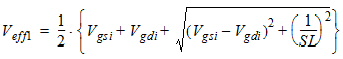
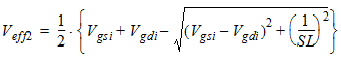
Materka Capacitance Model (CLVL=MAT)
When K1Vgsi < FCC
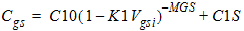
When K1Vgsi >= FCC
When K1Vgdi < FCC
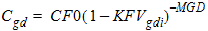
When K1Vgdi >= FCC
Raytheon Capacitance Model (CLVL=2)
Gate Charge
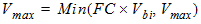
When Vnew
> Vmax

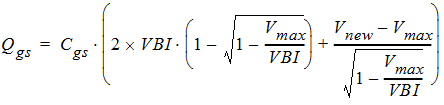
When Vnew
<= Vmax
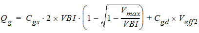
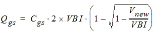
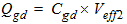
Where:
Temperature Effects
For all TMOD:

Quadratic Model, TMOD=0
Define:
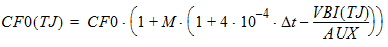
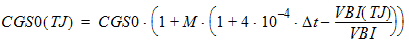
Dt = TJ - TNOM


Where Isat
= IG0 or IB0 and a
= ADAG or AFAB for the forward diode and breakdown efffects, respectively.

Where Vbi
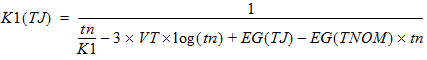
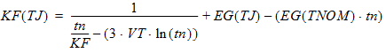
is 1/K1 or 1/KF.
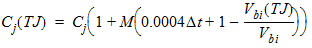
Where Cj is
C10 or CF0.
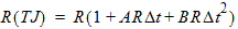
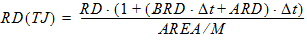
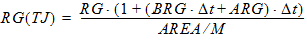
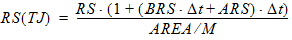
Where R is R10, RG, RD, or RS; AR and BR are the linear
and quadratic temperature coefficients for the respective resistances.
Materka Model, TMOD=0, CLVL=1


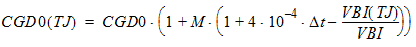
Raytheon Model, TMOD=0, CLVL=2


Linear Model, TMOD=1
This model for the temperature dependence modifies diode
saturation current using a physics-based equation and modifies several
of the model coefficients using a linear function of Dt. The model is an extension of the paper
by Anholt and Swirhun [2].

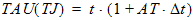
Where Isat
= IG0 or IB0 and a
= ADAG or AFAB for the forward diode and breakdown efffects, respectively.

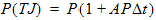
Where P is a parameter (e.g., RG, RD, or C10) and AP
is the temperature linear coefficient of that parameter (e.g., ARG,
ARD, or AC10).
The Linear temperature coefficient for VMAX is calculated
as


Materka Model, TMOD=1, CLVL=1:
Raytheon Model TMOD=1, CLVL=2:


References
1. A. Materka and T. Kacprzak, “Computer
calculation of large-signal GaAs FET amplifier characteristics,”
IEEE Transactions on Microwave Theory Tech., Vol. MTT-33, No. 2, pp.
129-135 Feb. 1985.
2. R.E. Anholt and S. E. Swirhun, “Experimental
Investigation of the Temperature Dependence of GaAs FET Equivalent Circuits,”
IEEE Trans. on ED, vol. 39, no. 9, pp. 2029-2036, Sept. 1992.


HFSS视频教程
ADS视频教程
CST视频教程
Ansoft Designer 中文教程
|