|
微波射频仿真设计 |
|
|
微波射频仿真设计 |
|
| 首页 >> Ansoft Designer >> Ansoft Designer在线帮助文档 |
|
Nexxim Simulator > Via Hole
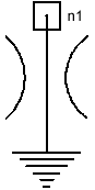
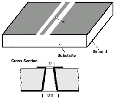 Netlist FormatAn instance of a grounded coplanar waveguide via hole has the following netlist syntax: Axxx n1 D=val DG=val COMPONENT=gcpw_viahole SUBSTRATE=substrate_name n1 is the name of the node attached to the via. The entry COMPONENT=gcpw_viahole identifies the element as a grounded coplanar waveguide via hole. The SUBSTRATE=substrate_name is the grounded coplanar waveguide substrate model name selected for the design (see Selecting a Grounded Coplanar Waveguide Substrate for details).
Netlist ExampleA23 Port1 D=3.0e-4 DG=5.0e-4 where GCPW1, the selected layout technology or substrate type, has a definition such as: .SUB GCPW1 GCPW( Notes1. Conditions for ±2%
accuracy of the no radiation loss model:
HFSS视频教程 ADS视频教程 CST视频教程 Ansoft Designer 中文教程 |
|
Copyright © 2006 - 2013 微波EDA网, All Rights Reserved 业务联系:mweda@163.com |
|


