| กก | |
| กก |
ฮขฒจษไฦตทยีๆษ่ผฦ |
| กก |
Agilent ADS สำฦตลเัตฝฬณฬ | CSTฮขฒจนคื๗สาสำฦตฝฬณฬ | AWR Microwave Office |
| กก | |
| กก |
ฮขฒจษไฦตทยีๆษ่ผฦ |
| กก |
Agilent ADS สำฦตลเัตฝฬณฬ | CSTฮขฒจนคื๗สาสำฦตฝฬณฬ | AWR Microwave Office |
| สืาณ >> Ansoft Designer >> Ansoft Designerิฺฯ฿ฐ๏ึ๚ฮฤตต |
|
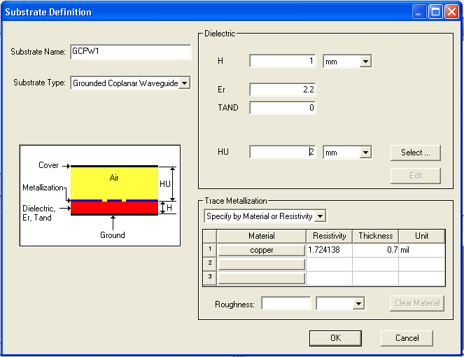
Nexxim Simulator > Creating a Custom Grounded Coplanar Waveguide SubstrateTo create a grounded coplanar waveguide substrate definition, open the Nexxim design icon (“Nexxim1” for example), then right-click on the Data field. Select Add Substrate Definition from the pulldown. The Substrate Definition window opens. Specify the name of your new substrate (the example below uses the name “GCPW1”):
Select Grounded Coplanar Waveguide as the Substrate Type. Complete the specifications for the Dielectric and the Trace Metallization. Refer to the Grounded Coplanar Waveguide (CPW) Substrate help topic for guidelines on defining grounded coplanar waveguide substrates. When the substrate definition is complete, click OK. If you selected None for the global substrate type in the Choose Layout Technology dialog, the custom offset stripline substrate becomes the global substrate type. When an element is instantiated , it includes a SUBSTRATE=substrate_name entry in its netlist syntax. Designer automatically inserts the global substrate_name into the internal netlist entry for the instantiated element.
HFSSสำฦตฝฬณฬ ADSสำฦตฝฬณฬ CSTสำฦตฝฬณฬ Ansoft Designer ึะฮฤฝฬณฬ |
กก |
|
Copyright © 2006 - 2013 ฮขฒจEDAอ๘, All Rights Reserved าตฮ๑มชฯตฃบmweda@163.com |
|