|
微波射频仿真设计 |
|
|
微波射频仿真设计 |
|
| 首页 >> Ansoft Designer >> Ansoft Designer在线帮助文档 |
|
Nexxim Simulator > Unmitered Bend, Gap Width
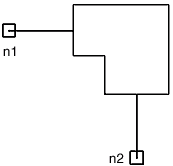 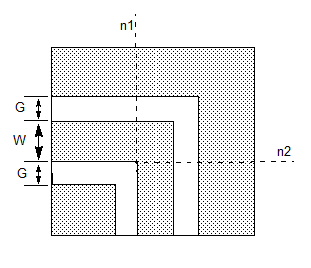 Netlist FormatAn instance of a grounded coplanar waveguide unmitered bend, gap width, has the following netlist syntax: Axxx n1 n2 [W=val] [G=val]
n1 and n2 are the names of the nodes attached to the bend. The entry COMPONENT=gcpw_unmitered_bend identifies the element as a grounded coplanar waveguide unmitered bend, gap width specified. The SUBSTRATE=substrate_name is the grounded coplanar waveguide substrate model name selected for the design (see Selecting a Grounded Coplanar Waveguide Substrate for details).
Netlist ExampleA5 Port1 Port2 W=0.75e-3
G=1.1e-3 where GCPW1, the selected layout technology or substrate type, has a definition such as: .SUB GCPW1 GCPW( Notes1. Reference planes coincide with the inside vertex of the corner, as shown in the figure. 2. For accurate results, the substrate definition
should specify: 3. The coplanar mode is assumed to exist only. Parasitic effects due to air bridges are not considered by this model.
HFSS视频教程 ADS视频教程 CST视频教程 Ansoft Designer 中文教程 |
|
Copyright © 2006 - 2013 微波EDA网, All Rights Reserved 业务联系:mweda@163.com |
|


