|
 Ansoft Designer / Ansys Designer 在线帮助文档: Ansoft Designer / Ansys Designer 在线帮助文档:
Nexxim Simulator >
Nexxim Component Models >
IBIS Buffer Elements >
Input/Output Buffer
Input/Output Buffer
Netlist Syntax
B_IOxxx nd_pu nd_pd nd_out nd_in nd_en
nd_out_of_in [nd_pc nd_gc]
+ file='file_name' model='model_name'
+ buffer=3|input_output
+ [typ=typ|min|max|fast|slow]
+ [power=on|off]
+ [interpol=1|2]
+ [nowarn]
+ [xv_pu=state_pu] [xv_pd=state_pd]
+ [ramp_fwf=2|1|0] [ramp_rwf=2|1|0]
+ [fwf_tune=fwf_tune_value] [rwf_tune=rwf_tune_value]
+ [c_com_pu=c_com_pu_fraction]
+ [c_com_pd=c_com_pd_fraction]
+ [c_com_pc=c_com_pc_fraction]
+ [c_com_gc=c_com_gc_fraction]
+ [pu_scal=pu_scal_value]
+ [pd_scal=pd_scal_value]
+ [pc_scal=pc_scal_value]
+ [gc_scal=gc_scal_value]
+ [rwf_scal=rwf_scal_value]
+ [fwf_scal=fwf_scal_value]
+ [spu_scal=spu_scal_value]
+ [spd_scal=spd_scal_value]
+ [rm_dly_rwf=rm_dly_rwf_value]
+ [rm_dly_fwf=rm_dly_fwf_value]
+ [rm_tail_rwf=rm_tail_rwf_value]
+ [rm_tail_rwf=rm_tail_fwf_value]
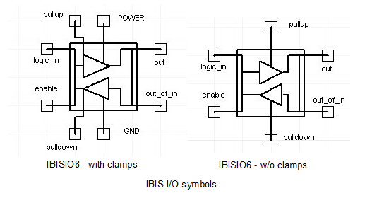
Node nd_pu is the pullup, nd_pd is the
pulldown, nd_in is the logic input, nd_out is the output,
nd_en is the enable, nd_out_of_in is the digital output
that responds to changes at the input. Node nd_pc is the power
clamp, nd_gc is the ground clamp, when present.
IBIS I/O BufferInstance
Parameters
Parameter
|
Description
|
Units
|
Default
|
FILE
|
Name of IBIS file
|
None
|
None
|
MODEL
|
Name of model in IBIS file. The
model type must match the instance type.
|
None
|
None
|
BUFFER
|
Code or token for buffer type.
Must be 3 or input_output for the Input/Output Buffer
type
|
None
|
None
|
TYP
|
Parameter range:
typ=midrange of all values
min=minimum of all values
max=maximum of all values
fast=maxima and minima selected to produce
the fastest transitions.
slow=maxima and minima selected to produce
the slowest transitions.
See TYP Parameter Effects for all
IBIS Buffers for fast and slow settings.
|
None
|
typ
|
POWER
|
Power mode:
on=PULLUP, PULLDOWN, POWER, and GND, as applicable,
are connected internally. The circuit must not connect voltage sources
to these terminals
off=Circuit must provide voltages to these
terminals
|
None
|
on
|
INTERPOL
|
Interpolation: 1=linear, 2=spline
|
None
|
1
|
NOWARN
|
When present, disable parser warnings
|
None
|
Warnings enabled
|
XV_PU
|
Name of node for pullup scaling
factor output
|
None
|
None
|
XV_PD
|
Name of node for pulldown scaling
factor output
|
None
|
None
|
RAMP_FWF
|
Falling waveform ramp specification:
0=ramp only, 1=single waveform in IBIS file, 2=double waveform in IBIS
file
|
None
|
2
|
RAMP_RWF
|
Rising waveform ramp specification:
0=ramp only, 1=single waveform in IBIS file, 2=double waveform in IBIS
file
|
None
|
2
|
FWF_TUNE
|
Falling waveform adjustment.
Used only when RAMP_FWF=0 or 1. Waveform assumes
device transitions from on to off in the fraction of the total transition
time given by FWF_TUNE.
|
None
|
0.1
|
RWF_TUNE
|
Rising waveform adjustment.
Used only when RAMP_RWF=0 or 1. Waveform assumes
device transitions from off to on in the fraction of the total transition
time given by RWF_TUNE.
|
None
|
0.1
|
C_COM_PC
|
Fraction of capacitance on power
clamp vs. GC, PU, and PD, (value between 0 and 1). Capacitance fractions
must sum to 1.0.
|
None
|
0
|
C_COM_GC
|
Fraction of capacitance on ground
clamp vs. PC, PU, and PD(value between 0 and 1). Capacitance fractions
must sum to 1.0.
|
None
|
1
|
C_COM_PU
|
Fraction of capacitance on pullup
vs. GC, PC, and PD (value between 0 and 1). Capacitance fractions must
sum to 1.0.
|
None
|
0
|
C_COM_PD
|
Fraction of capacitance on pulldown
vs. PC, GC, and PU (value between 0 and 1). Capacitance fractions must
sum to 1.0.
|
None
|
1
|
PC_SCAL
|
Scale factor for power clamp current
drive strength applied to IBIS table values
|
None
|
1.0
|
GC_SCAL
|
Scale factor for ground clamp current
drive strength applied to IBIS table values
|
None
|
1.0
|
PU_SCAL
|
Scale factor for pullup current
drive strength applied to IBIS table values
|
None
|
1.0
|
PU_SCAL
|
Scale factor for pulldown current
drive strength applied to IBIS table values
|
None
|
1.0
|
FWF_SCAL
|
Scale factor applied to falling
ramp transition time
|
None
|
1.0
|
RWF_SCAL
|
Scale factor applied to rising
ramp transition time
|
None
|
1.0
|
SPD_SCAL
|
Scale factor for pulldown current
drive strength applied to IBIS table values
Used only when POWER=OFF and the voltage difference
between the pullup and pulldown nodes is not equal to the [Voltage Range]
value in the IBIS file.
|
None
|
1.0
|
SPU_SCAL
|
Scale factor for pullup current
drive strength applied to IBIS table values
Used only when POWER=OFF and the voltage difference
between the pullup and pulldown nodes is not equal to the [Voltage Range]
value in the IBIS file.
|
None
|
1.0
|
RM_DLY_RWF
|
Amount of time to trim off the
front of the rising waveform, relative to time=0
|
Sec
|
0.0
|
RM_DLY_FWF
|
Amount of time to trim off the
front of the falling waveform, relative to time=0
|
Sec
|
0.0
|
RM_TAIL_RWF
|
Amount of time to trim off the
end of the rising waveform, relative to the time of the last point in
the waveform
|
Sec
|
0.0
|
RM_TAIL_FWF
|
Amount of time to trim off the
end of the falling waveform, relative to the time of the last point
in the waveform
|
Sec
|
0.0
|
Notes
[1] If any of the parameters RM_DLY_RWF, RM_DLY_FWF,
RM_TAIL_RWF, or RM_TAIL_FWF is given a negative value, Nexxim sets the
value to 0.0 with a warning.
[2] If the values of RM_DLY_RWF and RM_DLY_FWF
are not equal, Nexxim generates a warning, since the unequal values
alter the duty cycle of the output waveform relative to what is specified
by the IBIS file itself. The simulation will run.
[3] If the value of RM_DLY_RWF, RM_DLY_FWF, RM_TAIL_RWF,
or RM_TAIL_FWF is such that more than 10 percent of the original voltage
transition is trimmed off, Nexxim generates a warning, but the
simulation will run.
[4] If the values of RM_DLY_RWF and RM_TAIL_RWF
are such that fewer than three (3) data points are left in the resulting
waveform, Nexxim ignores the settings and issues a warning. With fewer
than three data points, ramp transitions may give better results.
[5] If the values of RM_DLY_FWF and RM_TAIL_FWF
are such that fewer than three (3) data points are left in the resulting
waveform, Nexxim ignores the settings and issues a warning. With fewer
than three data points, ramp transitions may give better results.
[6] If the sum of RM_DLY_RWF and RM_TAIL_RWF is
such that the entire rising waveform is removed, Nexxim halts
with an error.
[7] If the sum of RM_DLY_FWF and RM_TAIL_FWF is
such that the entire falling waveform is removed, Nexxim halts
with an error.


HFSS视频教程
ADS视频教程
CST视频教程
Ansoft Designer 中文教程
|