|
微波射频仿真设计 |
|
|
微波射频仿真设计 |
|
| 首页 >> Ansoft Designer >> Ansoft Designer在线帮助文档 |
|
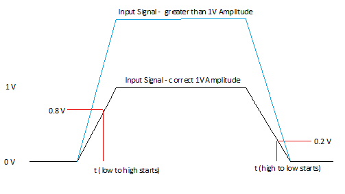
Nexxim Simulator > IBIS Buffer ConventionsThis section provides details on the conventions that should be followed to produce a correct simulation with the IBIS buffer elements. Power ParameterAll active IBIS components contains some combination of pullup, pulldown, power clamp, and ground clamp nodes. These components also have a configuration parameter power. By default, power is set to “on,” so that the component automatically drives the nodes using internal voltage sources set to the voltages specified in the IBIS model. When power is set to “on,” the user should NOT connect any of these nodes to voltage sources or to ground. Connecting external voltage sources or grounds when power is set to “on” generates warning messages about parallel supplies, and may cause problems with simulation. To use external sources and grounds, set the power parameter to “off.” With this setting, Nexxim expects all pullup, pulldown, power clamp, and ground clamp nodes to have the correct external voltages connected. Digital NodesAll digital nodes on IBIS components expect a voltage range of 0V to 1V. Input NodesDigital input nodes for drivers (output, I/O, etc.) use fixed thresholds of 0.2V and 0.8V to trigger changes in state from high to low and low to high, respectively. (Refer to diagram below).
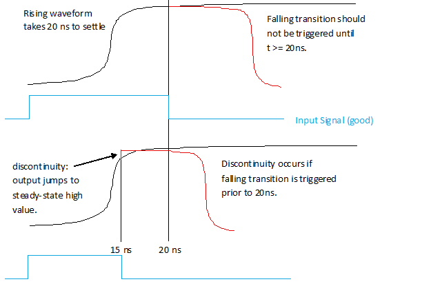
Any voltage supply may be connected to these nodes, but the expected values are 0V for low or off and 1V for high or on. Because the transition trigger thresholds are fixed, duty cycle distortion (DCD) occurs if a high amplitude other than 1Vis used (blue trace in diagram). The amount of DCD is negligible if the transitions themselves are very fast relative to the overall pulse width. Using a high amplitude of less than 0.8V results in no output transitions occurring. For initial transient values, and for DC analysis, a single fixed input threshold of 0.5V is used. If the input signal is above 0.5V, the output is placed in the high state. Otherwise, the output is placed in the low state. These descriptions of the relationships between input voltage and output state for the Input buffer nodes assume that Polarity parameter in the IBIS model is set to “Non-Inverting”. The relationships are appropriately inverted if the IBIS buffer model has Polarity defined as “Inverting.” Output NodesThe digital output nodes of receivers provide a waveform that switches between 0V and 1V. These transitions depend on the input signal and on the values of Vinl, Vinh, and Polarity set in the IBIS model. If the output is in the low state (0V) and the input signal becomes greater than Vinh, the output transitions to high (1V). If the output state is high (1V) and the input signal becomes less than Vinl, the output transitions to low (0V). For initial transient values, and for DC analysis, the buffers use a single fixed threshold equal to the average of Vinl and Vinh [(Vinh + Vinl)/2]. If the input signal is above this threshold, the output is placed in the high state (1V). Otherwise, the output is placed in the low state (0V). These descriptions of the relationships between input voltage and output state for the Output buffer nodes assume that Polarity parameter in the IBIS model is set to “Non-Inverting”. The relationships are appropriately inverted if the IBIS buffer model has Polarity defined as “Inverting.” Enable NodesA single fixed threshold of 0.5V is used for Enable nodes. If the Enable pin is higher than 0.5V, the enable state is considered high. Other wise, the enable state is considered low. The behavior of the component then depends on whether the IBIS buffer model has its Enable parameter set to “Active-High” or “Active-Low.” Avoid Overclocking DriversBe careful to ensure that the frequency of the input signal does not exceed the capabilities of the IBIS model. The frequency of the input signal must consider the time required for the output to settle. Whenever a transition from high to low or from low to high is triggered by the input signal, the output jumps immediately to the steady-state voltage value from which the next transition starts. However, the actual waveform requires a settling time period to reach the steady-state high or low voltage. If the input then changes state too soon, the next transition will occur before the initial transition has settled to its steady-state value. This can lead to discontinuities and other unexpected simulation results.
For example, if the IBIS model takes 20ns to complete a rising transition, then the input signal should stay in the high state (1V) for at least 20ns after a low-to-high-transition. If instead the input goes back to low after only 15ns, the behavior at the high-to-low transition creates a discontinuity in the output signal. Since the initial rising transition has not completed at 15ns, the output has not settled at the steady state from which the falling transition is to occur. The too-early falling transition causes the output to jump discontinuously to the high value. Buffer Import vs. Pin Import (pkg_selector)IBIS devices are created in Designer using either “Buffer Import” or “Pin Import.” A buffer import captures the behavior of a given model in an IBIS file. A Pin Import captures the behavior of a given pin on a component defined in the IBIS file. A device created via Pin Import contains the behavior of the model associated with the pin, and it also contains information about the parasitic package model specified for that pin. A device created with a Pin Import has functionality similar to one created via Buffer Import, but with an additional parameter pkg_selector. The pkg_selector parameter is used to select the desired packaging model. When pkg_selector is set to “Package,” the default package model for that component is used. When pkg_selector is set to “Pin,” the pin-specific package model is used if it exists, otherwise the default package model for that component is used. . When pkg_selector is set to “None,” no package model is used, and the device behavior is identical to one created with a Buffer Import of the same model.
HFSS视频教程 ADS视频教程 CST视频教程 Ansoft Designer 中文教程 |
|
Copyright © 2006 - 2013 微波EDA网, All Rights Reserved 业务联系:mweda@163.com |
|