|
微波射频仿真设计 |
|
|
微波射频仿真设计 |
|
| 首页 >> Ansoft Designer >> Ansoft Designer在线帮助文档 |
|
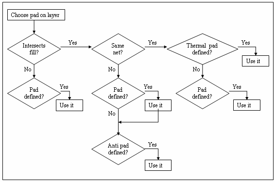
Using Component Libraries > Pad Behavior in Vias and PinsThe pad(s) used in a particular via/pin are determined by the padstack definition and by the intersected primitives in their nets. Multiple pads are sometimes defined for the same layer. • The intersection point between the central axis of a via/pin and the intersected layers is inspected to determine its metal type (fill, trace, or unpresent). By definition, ground layers are fill-metal with primitives defining scratch areas. • If a fill is intersected, the net of the fill is also taken into consideration. • Based on the intersection of the fill/net/pads that are defined in the padstack definition, the choice of pad that is used is determined using the following algorithm:

HFSS视频教程 ADS视频教程 CST视频教程 Ansoft Designer 中文教程 |
|
Copyright © 2006 - 2013 微波EDA网, All Rights Reserved 业务联系:mweda@163.com |
|