|
微波射频仿真设计 |
|
|
微波射频仿真设计 |
|
| 首页 >> Ansoft Designer >> Ansoft Designer在线帮助文档 |
|
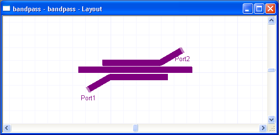
The Designer Desktop > Layout Editor WindowThe layout editor shows the physical realization of the circuit.
Components such as transmission lines will be drawn on the metal layer. Components that do not have footprints, such as ideal capacitors, will be represented in the layout as schematic symbols to indicate that no footprints are associated with them. Arbitrary graphical primitives unrelated to modeled elements can also be drawn. When components with footprints are added to a layout or modified, their footprint connection points may no longer be properly aligned with those of other components. To correct this misalignment, click Align Mw Ports on the Draw menu. For more information, see Layout Editor.
HFSS视频教程 ADS视频教程 CST视频教程 Ansoft Designer 中文教程 |
|
Copyright © 2006 - 2013 微波EDA网, All Rights Reserved 业务联系:mweda@163.com |
|